STM32F4 Embedded Rust at the PAC: System Clock Configuration

I am an 📟 Embedded Engineer with years of experience in both industry 🏭 and academia 🏫. Passionate Mentor 👨💼 and Instructor 👨🏫.
Aspiring Rustacean 🦀
This blog post is the third of a multi-part series of posts where I explore various peripherals in the STM32F401RE microcontroller using embedded Rust at the PAC level.
Prior posts include (in order of publishing):
🎬 Introduction
Configuring clocks is an essential part of any microcontroller system. There are various sources from which internal clocks can be generated. In turn, internal clocks drive various peripherals and buses. As such, ahead of dealing with posts that involve clock aspects like timers or serial communication, I figured this is a crucial post to lead with. Especially since the STM32 clock tree involves quite some detail. To make things easier, I'll be using the ST-Microelectronics CubeMX to help determine the frequencies we need and then configure the controller accordingly. To make sure the clocks have been configured I'm going to turn on the LED as a visual confirmation.
📚 Knowledge Pre-requisites
To understand the content of this post, you need the following:
Basic knowledge of coding in Rust.
Familiarity with the basic template for creating embedded applications in Rust.
💾 Software Setup
All the code presented in this post in addition to instructions for the environment and toolchain setup is available on the apollolabsdev Nucleo-F401RE git repo. Note that if the code on the git repo is slightly different then it means that it was modified to enhance the code quality or accommodate any Rust updates.
🛠 Hardware Setup
🧰 Materials

🔌 Connections
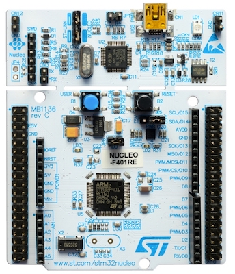
There will be no need for external connections. On-board connections will be utilized and include the following:
- An LED is connected to pin PA5 on the microcontroller. The pin will be used as an output.
👨🎨 Software Design
There isn't much of an application to design in this post. It's all configuration. Once the clock configuration is completed, the onboard LED will be activated. The LED activation is similar to the post from last week.
The STM32 microcontroller has several clocks that are used to operate different parts of the system. The main clocks on an STM32 microcontroller are:
HSE (High-Speed External) clock: This is an external clock signal that is connected to the microcontroller. It is typically a crystal oscillator and is used as the main clock source for the microcontroller.
HSI (High-Speed Internal) clock: This is an internal clock source that is built into the microcontroller. It is used as a backup clock source in case the HSE clock fails.
LSE (Low-Speed External) clock: This is an external clock signal that is used to drive the real-time clock (RTC) module in the microcontroller.
LSI (Low-Speed Internal) clock: This is an internal clock source that is built into the microcontroller. It is used to provide a low-power clock source for the microcontroller's internal circuits when the main clock is turned off.
PLL (Phase-Locked Loop) clock: This is a clock that is generated by multiplying the frequency of the HSE or HSI clock. It is used to provide a higher frequency clock for the microcontroller's core and peripherals.
The system clock of the STM32 microcontroller is generated by one of these clocks, which is selected by the microcontroller's internal clock control unit (RCC). The STM32F4 clock tree shows how these clocks are connected inside the controller. Additionally, the clock tree shows the different clock scaling options. From the STM32F4 reference manual the clock tree looks something as follows:

It's obvious that there are a lot of options to choose from. Additionally, one must take care as not all clock configuration options are compatible. To make this easier, we can use CubeMX. CubeMX is a graphical user interface (GUI) tool that is used to configure and generate initialization code for microcontroller projects based on STM32 microcontrollers. It is developed by STMicroelectronics and provides a user-friendly interface for configuring various peripherals and features of STM32 microcontrollers. In this case, we would be needing it to help us configure the clock tree. The nice thing also is that you can select which board you are using in CubeMX and it would automatically determine the external clocks.
Following that, I configured my clock treen in CubeMX as follows:

Note that all the greyed-out areas are ones we don't need to configure. On the other hand, what we will be configuring mainly are the Prescaler and multiplexer selections. To configure the clocks our code will take the following steps:
Enable the HSE and wait for it to become ready.
Configure the Prescalar value for HCLK, PCLK1, & PCLK2.
Configure the Main PLL.
Enable the PLL and wait for it to become ready.
Select the system clock source and wait for it to be set.
Turn on the LED to confirm completion.
In the next section, we'll elaborate further on the registers that need to be accessed as well.
👨💻 Code Implementation
📥 Crate Imports
In this implementation, three crates are required as follows:
The
cortex_m_rtcrate for startup code and minimal runtime for Cortex-M microcontrollers.The
panic_haltcrate to define the panicking behavior to halt on panic.The
stm32f4xx_paccrate to import the STM32F401 microcontroller device PAC API that was created in the first post in this series.
use cortex_m_rt::entry;
use panic_halt as _;
use stm32f401_pac as pac;
🎛 Peripheral Configuration Code
Here we need to follow the steps that were stated earlier in the software design, though an essential step is required first.
1- Obtain a Handle for the Device Peripherals: As we always do and part of the singleton pattern, this needs to be done before accessing any peripheral register. Here I create a device peripheral handler named dp as follows:
let dp = pac::Peripherals::take().unwrap();
Using this handle, I will be accessing the peripherals of the device.
2- Enable the HSE Clock and Wait for it to Become Ready: The HSE is configured through the RCC_CR register which has the following mapping (obtained from the STM32F4 reference manual):

Note that the HSE is enabled via bit 16 which is both read and write. Generally, when enabling a clock source, we also need to make sure that it's ready before proceeding. This is done via bit 17 for the HSE which is only read. As such, to enable the HSE and check if its ready we do the following:
dp.RCC.cr.write(|w| w.hseon().set_bit());
while dp.RCC.cr.read().hserdy().bit() {}
in the above code the while loop ensures that we do not proceed until the HSE RDY bit is asserted.
3- Configure the Prescalar value for HCLK, PCLK1, & PCLK2: Note from the earlier figure for the clock tree that I configured in CubeMX that I had Prescalar values of 1, 2, and 1 for HCLK, PCLK1, and PCLK2, respectively. These values are configured through the RCC clock configuration register RCC_CFGR :

Fields HPRE (bits 4-7) ,PPRE1 (bits 10-12), and PPRE2 (bits 13-15) are the ones we need to change. The value we should use is specified in the reference manual as well:


Looking at the values, only PCLK1 needs to be modified since we are not using a divide factor for the others. The default is not to divide the system clock (prescalar of 1) according to the reset value of the register. This results in the following line of code:
dp.RCC.cfgr.write(|w| unsafe { w.ppre1().bits(0b100) });
Here the code is considered unsafe because we could be writing a reserved bit pattern into the register field.
4- Configure the Main PLL: For this we need to configure the PLL source multiplexer (HSE or HSI), and also set the values for PLLM, PLLN and PLLP. This is all done via the PLL configuration register RCC_PLLCFGR :

Also according to the earlier values determined by CubeMX, this results in the following code:
    // Configure PLL M
    dp.RCC.pllcfgr.write(|w| {
        w.pllm5()
            .bit(false)
            .pllm4()
            .bit(false)
            .pllm3()
            .bit(true)
            .pllm2()
            .bit(false)
            .pllm1()
            .bit(false)
            .pllm0()
            .bit(false)
    });

    // Configure PLL N
    dp.RCC.pllcfgr.write(|w| {
        w.plln8()
            .set_bit()
            .plln7()
            .clear_bit()
            .plln6()
            .set_bit()
            .plln5()
            .clear_bit()
            .plln4()
            .set_bit()
            .plln3()
            .clear_bit()
            .plln2()
            .clear_bit()
            .plln1()
            .clear_bit()
            .plln0()
            .clear_bit()
    });

    // Configure PLL P
    dp.RCC
        .pllcfgr
        .write(|w| w.pllp0().bit(true).pllp1().bit(false));
5- Enable the PLL and wait for it to become ready: This is exactly the same process as the HSE earlier. However, we had to wait until we configure the PLL parameters before turning it on. Using the same RCC_CR register we used in step 1, we now turn on the PLL then wait as follows:
dp.RCC.cr.write(|w| w.pllon().set_bit());
while dp.RCC.cr.read().pllrdy().bit() {}
6- Select the System Clock Source and Wait for it to be Set: This is out final step in the configuration of the clock. This is about selecting the desired input for the system clock multiplexer. This is done through the RCC clock configuration register RCC_CFGR SWS and SW bits:

First we start by setting the SW bits and then wait for the status to indicate that the switch happened:
dp.RCC.cfgr.write(|w| w.sw1().set_bit().sw0().clear_bit());
while dp.RCC.cfgr.read().sws1().bit_is_set() && dp.RCC.cfgr.read().sws0().bit_is_clear() {}
7- Turn on the LED to confirm completion: Now that the configuration is over, we can turn on the LED to confirm the conclusion of the setup. The details of configuring GPIO was discussed in detail in the previous post resulting in the following code:
//Enable Clock to GPIOA
dp.RCC.ahb1enr.write(|w| w.gpioaen().set_bit());
//Configure PA5 as Output
dp.GPIOA.moder.write(|w| unsafe { w.moder5().bits(0b01) });
// Set PA5 Output to High signalling end of configuration
dp.GPIOA.odr.write(|w| w.odr5().set_bit());
This is it for configuration.
📱 Application Code
This post does not have an application. The purpose was only to configure clocks. We only need to include a loop construct that is empty as follows:
loop {}
📀 Full Application Code
Here is the full code for the implementation described in this post. You can additionally find the full project and others available on the apollolabsdev Nucleo-F401RE git repo.
#![no_std]
#![no_main]

// Imports
use cortex_m_rt::entry;
use panic_halt as _;
use stm32f401_pac as pac;

#[entry]
fn main() -> ! {
    // Setup handler for device peripherals
    let dp = pac::Peripherals::take().unwrap();

    // Enable HSE Clock
    dp.RCC.cr.write(|w| w.hseon().set_bit());

    // Wait for HSE clock to become ready
    while dp.RCC.cr.read().hserdy().bit() {}

    // Configure PCLK1 Prescalar
    dp.RCC.cfgr.write(|w| unsafe { w.ppre1().bits(0b100) });

    // Configure PLL M
    dp.RCC.pllcfgr.write(|w| {
        w.pllm5()
            .bit(false)
            .pllm4()
            .bit(false)
            .pllm3()
            .bit(true)
            .pllm2()
            .bit(false)
            .pllm1()
            .bit(false)
            .pllm0()
            .bit(false)
    });

    // Configure PLL N
    dp.RCC.pllcfgr.write(|w| {
        w.plln8()
            .set_bit()
            .plln7()
            .clear_bit()
            .plln6()
            .set_bit()
            .plln5()
            .clear_bit()
            .plln4()
            .set_bit()
            .plln3()
            .clear_bit()
            .plln2()
            .clear_bit()
            .plln1()
            .clear_bit()
            .plln0()
            .clear_bit()
    });

    // Configure PLL P
    dp.RCC
        .pllcfgr
        .write(|w| w.pllp0().bit(true).pllp1().bit(false));

    // Enable PLL
    dp.RCC.cr.write(|w| w.pllon().set_bit());

    // Wait for PLL to become ready
    while dp.RCC.cr.read().pllrdy().bit() {}

    // Select PLL as System Clock Source
    dp.RCC.cfgr.write(|w| w.sw1().set_bit().sw0().clear_bit());

    // Wait for PLL to be selected as System Clock Source
    while dp.RCC.cfgr.read().sws1().bit_is_set() && dp.RCC.cfgr.read().sws0().bit_is_clear() {}

    //Enable Clock to GPIOA
    dp.RCC.ahb1enr.write(|w| w.gpioaen().set_bit());

    //Configure PA5 as Output
    dp.GPIOA.moder.write(|w| unsafe { w.moder5().bits(0b01) });

    // Set PA5 Output to High signalling end of configuration
    dp.GPIOA.odr.write(|w| w.odr5().set_bit());

    loop {}
}
🔬 Further Experimentation/Ideas
- Use CubeMX to try out different clock configurations, then look into the reference manual and figure out how to use configure the registers accordingly.
Conclusion
In this post, Rust code was developed to configure clocks of an STM32 device exclusively at the peripheral access crate (PAC) level. The application was developed for an STM32F401RE microcontroller deployed on the Nucleo-F401RE development board. Have any questions? Share your thoughts in the comments below 👇.


